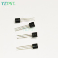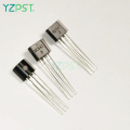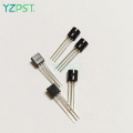

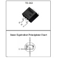

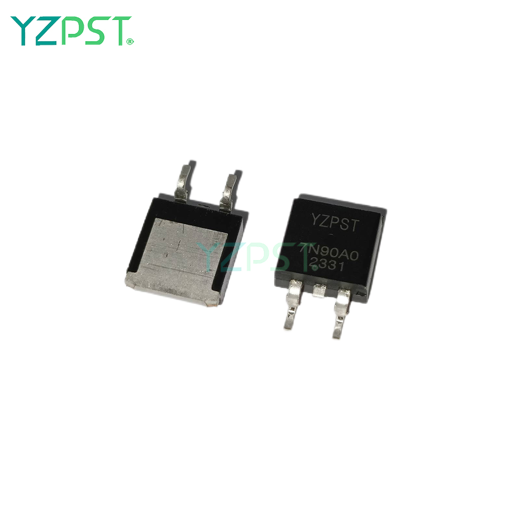
Chuyển đổi nhanh sang 263 7N90A0 Silicon N-Channel Power MOSFET
$0.452000-19999 Piece/Pieces
$0.35≥20000Piece/Pieces
| Hình thức thanh toán: | L/C,T/T,Paypal |
| Incoterm: | FOB,CFR,CIF |
| Giao thông vận tải: | Ocean,Land,Express,Others |
| Hải cảng: | SHANGHAI |

$0.452000-19999 Piece/Pieces
$0.35≥20000Piece/Pieces
| Hình thức thanh toán: | L/C,T/T,Paypal |
| Incoterm: | FOB,CFR,CIF |
| Giao thông vận tải: | Ocean,Land,Express,Others |
| Hải cảng: | SHANGHAI |
Mẫu số: YZPST-7N90A0
Thương hiệu: Yzpst
Nguồn Gốc: Trung Quốc
V DSS: 900V
ID: 7A
PD (TC =25℃): 160W
RDS(ON)TYP: 1.4Ω
A1 IDM: 28A
VGS: ±30V
A2 EAS: 700mJ
A1 EAR: 60mJ
| Đơn vị bán hàng | : | Piece/Pieces |
| Loại gói hàng | : | 1. Bao bì chống điện trường 2. hộp carton 3. bím tóc |
| Tải về | : |
|

Thử nghiệm năng lượng Avalanche Pulse 100%

| Symbol | Parameter | Rating | Units |
| V DSS | Drain-to- Source Voltage | 900 | V |
| ID | Continuous Drain Current | 7 | A |
| Continuous Drain Current TC = 100 °C | 5 | A | |
| a1 | Pulsed Drain Current | 28 | A |
| IDM | |||
| VGS | Gate-to-Source Voltage | ±30 | V |
| a2 | Single Pulse Avalanche Energy | 700 | mJ |
| EAS | |||
| a1 | Avalanche Energy , Repetitive | 60 | mJ |
| EAR | |||
| a1 | Avalanche Current | 2.4 | A |
| IAR | |||
| dv/dt | Peak Diode Recovery dv/dt | 5 | V/ns |
| a3 | |||
| PD | Power Dissipation | 160 | W |
| Derating Factor above 25 °C | 1.28 | W/℃ | |
| TJ ,Tstg | Operating Junction and Storage | 150 ,– 55 to 150 | ℃ |
| Temperature Range | |||
| TL | MaximumTemperature for Soldering | 300 | ℃ |
Đặc điểm điện CS (TC = 25 ℃ trừ khi có quy định khác)
| OFF Characteristics | ||||||
| Symbol | Parameter | Test Conditions | Rating | Units | ||
| Min. | Typ. | Max. | ||||
| V DSS | Drain to Source Breakdown | VGS =0V, I D =250µA | 900 | -- | -- | V |
| Voltage | ||||||
| ΔBVDSS/ ΔTJ | Bvdss Temperature Coefficient | ID=250uA, Reference25℃ | -- | 0.8 | -- | V/℃ |
| VDS = 900V, VGS = 0V, | -- | -- | 1 | |||
| IDSS | Drain to Source Leakage Current | Ta = 25℃ | µ A | |||
| VDS =720V, VGS = 0V, | -- | -- | 250 | |||
| Ta = 125℃ | ||||||
| IGSS( F) | Gate to Source Forward Leakage | VGS = +30V | -- | -- | 10 | µ A |
| IGSS(R ) | Gate to Source Reverse Leakage | VGS =- 30V | -- | -- | -10 | µ A |
| ON Characteristics | ||||||
| Symbol | Parameter | Test Conditions | Rating | Units | ||
| Min. | Typ. | Max. | ||||
| RDS(ON) | Drain-to-Source On- Resistance | VGS =10V, I D =3.0A | -- | 1.4 | 1.8 | Ω |
| VGS(TH ) | Gate Threshold Voltage | VDS = VGS, I D = 250µA | 2.5 | -- | 4.5 | V |
| Pulse width tp ≤380µs,δ≤2% | ||||||
| Dynamic Characteristics | ||||||
| Symbol | Parameter | Test Conditions | Rating | Units | ||
| Min. | Typ. | Max. | ||||
| gfs | Forward Transconductance | VDS = 15V, I D =3A | -- | 8 | -- | S |
| Ciss | Input Capacitance | -- | 1460 | -- | ||
| Coss | Output Capacitance | VGS = 0V VDS = 25V | -- | 130 | -- | pF |
| Crss | Reverse Transfer Capacitance | f = 1.0MHz | -- | 23 | -- | |
| Resistive Switching Characteristics | ||||||
| Symbol | Parameter | Test Conditions | Rating | Units | ||
| Min. | Typ. | Max. | ||||
| td(ON) | Turn-on Delay Time | -- | 22 | -- | ||
| tr | Rise Time | I D =7.0A V DD = 450V | -- | 45 | -- | |
| td(OFF ) | Turn-Off Delay Time | VGS = 10V RG = 9.1Ω | -- | 33 | -- | ns |
| tf | Fall Time | -- | 37 | -- | ||
| Qg | Total Gate Charge | -- | 37 | -- | ||
| Qgs | Gate to Source Charge | I D =7 . 0A V DD =450V | -- | 8 | -- | nC |
| Qgd | Gate to Drain (“ Miller ”)Charge | VGS = 10V | -- | 14 | -- | |


Điện thoại: 86-514-87782298
Whatsapp: +8613805278321
Địa chỉ: 3rd Floor, Weiheng Building No.20 B Area, Yangzhou, Jiangsu China
Trang web: https://vi.yzpst.com


Privacy statement: Your privacy is very important to Us. Our company promises not to disclose your personal information to any external company with out your explicit permission.
Fill in more information so that we can get in touch with you faster
Privacy statement: Your privacy is very important to Us. Our company promises not to disclose your personal information to any external company with out your explicit permission.