
Điều khiển pha bán dẫn 25TTS12 1200V
$0.252000-99999 Piece/Pieces
$0.22≥100000Piece/Pieces
| Hình thức thanh toán: | L/C,T/T,Paypal |
| Incoterm: | FOB,CFR,CIF |
| Đặt hàng tối thiểu: | 2000 Piece/Pieces |
| Giao thông vận tải: | Ocean,Air |
| Hải cảng: | SHANGHAI |

$0.252000-99999 Piece/Pieces
$0.22≥100000Piece/Pieces
| Hình thức thanh toán: | L/C,T/T,Paypal |
| Incoterm: | FOB,CFR,CIF |
| Đặt hàng tối thiểu: | 2000 Piece/Pieces |
| Giao thông vận tải: | Ocean,Air |
| Hải cảng: | SHANGHAI |
Mẫu số: YZPST-25TTS12-1
Thương hiệu: YZPST
| Đơn vị bán hàng | : | Piece/Pieces |
| Loại gói hàng | : | 1. Bao bì chống tĩnh điện 2. Hộp carton 3. Bao bì nhựa bảo vệ |
Điều khiển pha SCR, 25 A
MÔ TẢ / TÍNH NĂNG
25TTS ... Bộ chỉnh lưu điều khiển bằng silicon có điện áp cao được thiết kế đặc biệt cho các ứng dụng điều khiển pha và chuyển mạch công suất trung bình. Công nghệ thụ động thủy tinh được sử dụng có hoạt động đáng tin cậy lên đến
Nhiệt độ tiếp giáp 125 ° C.
Các ứng dụng điển hình là trong chỉnh lưu đầu vào (khởi động mềm) và các sản phẩm này được thiết kế để sử dụng với điốt, công tắc và bộ chỉnh lưu đầu vào Vishay có sẵn trong các phác thảo gói giống hệt nhau.
Sản phẩm này đã được thiết kế và đủ điều kiện cho trình độ công nghiệp.

|
PRODUCT SUMMARY |
|
|
VT at 16 A |
< 1.25 V |
|
ITSM |
300 A |
|
VRRM |
800/1200 V |
|
OUTPUT CURRENT IN TYPICAL APPLICATIONS |
|||
|
APPLICATIONS |
SINGLE-PHASE BRIDGE |
THREE-PHASE BRIDGE |
UNITS |
|
Capacitive input filter TA = 55 °C, TJ = 125 °C, common heatsink of 1 °C/W |
18 |
22 |
A |
|
MAJOR RATINGS AND CHARACTERISTICS |
|||
|
PARAMETER |
TEST CONDITIONS |
VALUES |
UNITS |
|
IT(AV) |
Sinusoidal waveform |
16 |
A |
|
IRMS |
|
25 |
|
|
VRRM/VDRM |
|
800/1200 |
V |
|
ITSM |
|
300 |
A |
|
VT |
16 A, TJ = 25 °C |
1.25 |
V |
|
dV/dt |
|
500 |
V/µs |
|
dI/dt |
|
150 |
A/µs |
|
TJ |
|
- 40 to 125 |
°C |
|
VOLTAGE RATINGS |
|||
|
PART NUMBER |
VRRM, MAXIMUM PEAK REVERSE VOLTAGE V |
VDRM, MAXIMUM PEAK DIRECT VOLTAGE V |
IRRM/IDRM AT 125 °C mA |
|
25TTS08 |
800 |
800 |
10 |
|
25TTS12 |
1200 |
1200 |
|
|
ABSOLUTE MAXIMUM RATINGS |
||||||
|
PARAMETER |
SYMBOL |
TEST CONDITIONS |
VALUES |
UNITS |
||
|
TYP. |
MAX. |
|||||
|
Maximum average on-state current |
IT(AV) |
TC = 93 °C, 180° conduction half sine wave |
16 |
A |
||
|
Maximum RMS on-state current |
IRMS |
|
25 |
|||
|
Maximum peak, one-cycle, non-repetitive surge current |
ITSM |
10 ms sine pulse, rated VRRM applied |
300 |
|||
|
10 ms sine pulse, no voltage reapplied |
350 |
|||||
|
Maximum I2t for fusing |
I2t |
10 ms sine pulse, rated VRRM applied |
450 |
A2s |
||
|
10 ms sine pulse, no voltage reapplied |
630 |
|||||
|
Maximum I2√t for fusing |
I2√t |
t = 0.1 to 10 ms, no voltage reapplied |
6300 |
A2√s |
||
|
Maximum on-state voltage drop |
VTM |
16 A, TJ = 25 °C |
1.25 |
V |
||
|
On-state slope resistance |
rt |
TJ = 125 °C |
12.0 |
mΩ |
||
|
Threshold voltage |
VT(TO) |
1.0 |
V |
|||
|
Maximum reverse and direct leakage current |
IRM/IDM |
TJ = 25 °C |
VR = Rated VRRM/VDRM |
0.5 |
mA |
|
|
TJ = 125 °C |
10 |
|||||
|
Holding current |
IH |
Anode supply = 6 V, resistive load, initial IT = 1 A |
- |
100 |
||
|
Maximum latching current |
IL |
Anode supply = 6 V, resistive load |
200 |
|||
|
Maximum rate of rise of off-state voltage |
dV/dt |
|
500 |
V/µs |
||
|
Maximum rate of rise of turned-on current |
dI/dt |
|
150 |
A/µs |
||
|
TRIGGERING |
||||
|
PARAMETER |
SYMBOL |
TEST CONDITIONS |
VALUES |
UNITS |
|
Maximum peak gate power |
PGM |
|
8.0 |
W |
|
Maximum average gate power |
PG(AV) |
|
2.0 |
|
|
Maximum peak positive gate current |
+ IGM |
|
1.5 |
A |
|
Maximum peak negative gate voltage |
- VGM |
|
10 |
V |
|
Maximum required DC gate current to trigger |
IGT |
Anode supply = 6 V, resistive load, TJ = - 10 °C |
60 |
mA |
|
Anode supply = 6 V, resistive load, TJ = 25 °C |
45 |
|||
|
Anode supply = 6 V, resistive load, TJ = 125 °C |
20 |
|||
|
Maximum required DC gate voltage to trigger |
VGT |
Anode supply = 6 V, resistive load, TJ = - 10 °C |
2.5 |
V |
|
Anode supply = 6 V, resistive load, TJ = 25 °C |
2.0 |
|||
|
Anode supply = 6 V, resistive load, TJ = 125 °C |
1.0 |
|||
|
Maximum DC gate voltage not to trigger |
VGD |
TJ = 125 °C, VDRM = Rated value |
0.25 |
|
|
Maximum DC gate current not to trigger |
IGD |
2.0 |
mA |
|
|
SWITCHING |
||||
|
PARAMETER |
SYMBOL |
TEST CONDITIONS |
VALUES |
UNITS |
|
Typical turn-on time |
tgt |
TJ = 25 °C |
0.9 |
µs |
|
Typical reverse recovery time |
trr |
TJ = 125 °C |
4 |
|
|
Typical turn-off time |
tq |
110 |
||
|
THERMAL AND MECHANICAL SPECIFICATIONS |
|||||
|
PARAMETER |
SYMBOL |
TEST CONDITIONS |
VALUES |
UNITS |
|
|
Maximum junction and storage temperature range |
TJ, TStg |
|
- 40 to 125 |
°C |
|
|
Maximum thermal resistance, junction to case |
RthJC |
DC operation |
1.1 |
°C/W |
|
|
Maximum thermal resistance, junction to ambient |
RthJA |
|
62 |
||
|
Typical thermal resistance, case to heatsink |
RthCS |
Mounting surface, smooth and greased |
0.5 |
||
|
Approximate weight |
|
|
2 |
g |
|
|
0.07 |
oz. |
||||
|
Mounting torque |
minimum |
|
|
6 (5) |
kgf · cm (lbf · in) |
|
maximum |
|
|
12 (10) |
||
|
Marking device |
|
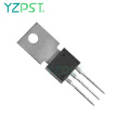
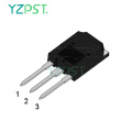
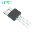
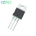
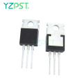
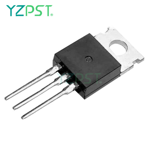
Case style TO-220AB |
25TTS08 |
||
|
25TTS12 |
|||||


Điện thoại: 86-514-87782298
Whatsapp: +8613805278321
Địa chỉ: 3rd Floor, Weiheng Building No.20 B Area, Yangzhou, Jiangsu China
Trang web: https://vi.yzpst.com


Privacy statement: Your privacy is very important to Us. Our company promises not to disclose your personal information to any external company with out your explicit permission.
Fill in more information so that we can get in touch with you faster
Privacy statement: Your privacy is very important to Us. Our company promises not to disclose your personal information to any external company with out your explicit permission.